



Infineon Technologies TLV55624-1O XENSIV™ TMR-Based Switch

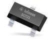
Infineon Technologies TLV55624-1O XENSIV™ TMR-Based Switch is an ultra-low-power, omnipolar switch with approximately 7nA typical current consumption in a duty-cycled operating mode, enabling a magnetic switch with almost zero power consumption. The switch operates over a 1.1V to 3.6V voltage range with an operating temperature from -40°C to +85°C. With its outstanding energy-saving design, the sensor is perfectly suited as a wake-up switch for ultra-low-power applications of any kind, and specifically for single-cell battery-powered applications with low supply voltages. The Infineon TLV55624-1O is assembled in a space-saving PG-XQFN-7-1 package.
Features
- Omnipolar magnetic switch
- Ultra-low ~7nA power consumption (at VDD = 1.55V; TAmb = +25°C; fs = 1.2Hz)
- 1.1V to 3.6V supply voltage range
- Capable of high output current to drive loads directly
- ±1.0mT operating point
- ±4.5mT release point
- Dedicated pins for extended functionalities
- Lock output state (LOCK pin)
- Force sensor to sleep mode (FSLP pin)
- Wide -40°C to +85°C operating temperature range
- Small PG-XQFN-7-1 package (1.50mm x 1.50mm x 0.38mm)
Applications
- Wake-up sensing for energy-constrained systems
- Medical devices
- Wearables
- IoT edge nodes
- Battery-powered products
- Low-energy utility infrastructure (smart metering and tamper detection)
- Always-on motion and event detection
Specifications
- 7.0nA to 50.0nA typical average supply current range
- 200.0µA typical transient peak supply current in measure mode
- 1µF typical recommended bypass capacitor
- LOCK time
- 0.5µs minimum setup
- 1.0µs minimum hold
- 1.0µs minimum FSLP pulse width
- 100.0ms maximum power-on time, 2.0ms typical
- 1.0ms to 4.0ms output rise time range
- 4.0ms maximum output fall time, 1.5ms typical
- 80.0ms to 750.0ms glitch filter time duration range
- Output resistance
- 5.0Ω maximum on, 2.0Ω typical
- 350.0Ω maximum off, 80.0Ω typical
- 1.0mT to 5.0mT magnetic hysteresis range
- 0.4Hz to 2.4Hz magnetic sample rate range
- ESD protection
- ±2.0kV Human Body Model voltage range
- ±500.0V Charged-Device Model voltage range
- 112K/W to 168.0K/W ambient junction thermal resistance range
Functional Block Diagram

Basic Application Circuitry

Example Application Diagram

Related Switches
Infineon Technologies XENSIV™磁霍尔开关
广泛的小尺寸封装产品组合,其电流消耗可降低10%。
发布日期: 2026-09-09
| 更新日期: 2026-09-09