Analog Devices Inc. AD7172-4 低功耗 Σ-Δ 模数转换器
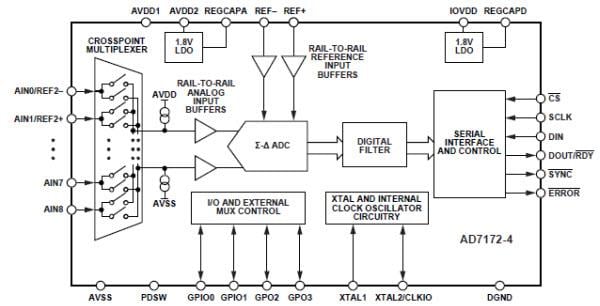
亚德诺半导体 AD7172-4 低功耗 Σ-Δ 模数转换器(ADC)是低功耗、多路复用 Σ-Δ ADC,具有 4 或 8 通道(全差分/单端)输入,可供低带宽信号使用。扫描全稳定数据时,AD7172-4 的最大通道扫描速率可达 6.21kSPS (161μs)。输出数据速率范围从 1.25SPS 至 31.25kSPS。AD7172-4 模数转换器集成了重要的模拟和数字信号调理块,设计人员能够通过 SPI 单独配置使用中的每一模拟输入通道。模拟输入和基准输入上的集成式真轨到轨缓冲器方便驱动高输入阻抗。AD7172-4 数字滤波器以 27.27SPS 的输出数据速率达到了 50Hz 和 60Hz 的同步抑制。设计人员可根据应用中每个通道的具体需要而在不同滤波器选项之间进行切换。其他数字处理功能包括失调和增益校准寄存器,可根据各通道进行配置。通用输入/输出(GPIO)控制外部多路复用器,实现其与模数转换器转换时间的同步。AD7172-4 ADC 采用 5mm × 5mm 的 32 引脚 LFCSP 封装,额定工作于 40°C 到 +105°C 温度范围内,很适合用于 PLC/DCS 模块,面向过程控制、温度& 压力测量、医疗 & 科学多通道仪器仪表和色层分析等应用。The AD7172-4 ADCs integrate key analog and digital signal conditioning blocks to allow designers to configure an individual setup for each analog input channel in use via the SPI. Integrated true rail-to-rail buffers on the analog inputs and reference inputs provide easy-to-drive high impedance inputs. AD7172-4's digital filter enables simultaneous 50Hz and 60Hz rejection at a 27.27SPS output data rate. The designer can switch between different filter options according to the demands of each channel in the application. Additional digital processing functions such as offset and gain calibration registers are configurable on a per-channel basis. General-purpose input/outputs (GPIOs) control external multiplexers synchronous to the ADC conversion timing.
Available in a 5mm × 5mm, 32-lead LFCSP package and specified for an operating temperature range of 40°C to +105°C, the AD7172-4 ADCs are well-suited for PLC/DCS modules for process control, temperature & pressure measurement, medical & scientific multi-channel instrumentation, and chromatography.
Analog Devices offers the EVAL-AD7172-4SDZ evaluation kit to help designers evaluate the features of the AD7172-4 ADC.
特性
- Fast and flexible output rate: 1.25SPS to 31.25kSPS
- Channel scan data rate of 6.21kSPS/channel (161μs settling)
- Performance specifications
- 17.2 noise-free bits at 31.25kSPS
- 24 noise-free bits at 5SPS
- INL: ±2ppm of FSR
- 85dB rejection of 50Hz and 60Hz with 50ms settling
- User-configurable input channels
- 4 fully-differential channels or 2 single-ended channels
- Crosspoint multiplexer
- Internal or external clock
- True rail-to-rail analog and reference input buffers
- Power supply
- AVDD1 = 3.0V to 5.5V, AVDD2 = IOVDD = 2V to 5.5V
- Split supply with AVDD1 and AVSS at ±2.5V or ±1.65V
- ADC current: 1.5mA
- Temperature range: −40°C to +105°C
- 3- or 4-wire serial digital interface (Schmitt trigger on SCLK) Serial port interface (SPI), QSPI-, MICROWIRE-, and DSP compatible
应用
- Process control
- PLC/DCS modules
- Temperature and pressure measurement
- Medical and scientific multi-channel instrumentation
- Chromatography
Functional Block Diagram


