Analog Devices Inc. ADA4807-1/-2 运算放大器
亚德诺半导体 ADA4807-1 单通道和 ADA4807-2 双通道运算放大器是低功耗、低噪声、轨到轨电压反馈放大器,具有极高的性能。它们被设计为业界具有最低输入噪声(3.1nV/√Hz 和 0.7pA/√Hz)的运放,同时工作静态电源电流仅为 1mA 或更低。低静态电流工作使 ADA4807-1/ADA4807-2 适用于从电池供电的便携式仪器到器件密度要求具有更低功耗的高速系统等各种应用。 ADA4807-1/ADA4807-2 运放具有较宽的电源电压范围,从±1.5V 至±5V, 采用 3V 至 10V 单电源供电。该运放具有禁用特性,置位时可将典型静态电源电流降低至 2.4μA。ADA4807-1/ADA4807-2 运放工作在 -40°C 到 +125°C 的工业温度范围,具有高速性能,−3dB 小信号带宽为 200MHz,压摆率为 225V/µs,0.1% 建立时间为 47ns(4V 步进),低输入失调电压为 ±20μV,漂移为 0.7 μV/°C 。对于 ±5V 电源,用 2Vp-p、100kHz 输出信号驱动 1 kΩ 负载时,HD2 为 −112dBc,HD3 为–115dBc。低失真和快速建立时间使 ADA4807-1/ADA4807-2 运放非常适合驱动最高 18 位分辨率的高速单电源精密模数转换器。应用包括高速、电池供电系统、高器件密度系统、高分辨率模数转换器(ADC)驱动器、便携式测试仪器和有源滤波器。ADA4807-1(单通道)采用节约空间的 6 引脚 SC70 和 6 引脚 SOT-23 封装,而 ADA4807-2(双通道)采用 10 引脚 LFCSP 和 8 引脚 MSOP 封装。The ADA4807-1/ADA4807-2/ADA4807-4 op-amps operate over a wide range of supply voltages from ±1.5V to ±5V, as well as from 3V to 10V single supplies. The op-amps include a disable feature to reduce the typical quiescent supply current to 2.4μA or less when asserted.
Operating over the -40°C to +125°C industrial temperature range, ADA4807-1/ADA4807-2/ADA4807-4 op-amps deliver a high-speed performance of 180MHz with small signal −3 dB bandwidth, a 225V/μs slew rate, and a settling time of 47ns to 0.1% (4V step) with a low input offset voltage of ±20μV and 0.7 μV/°C drift. For ±5V supplies, the HD2 is −112dBc and HD3 is -115dBc for a 2Vp-p, 100kHz output signal driving a 1 kΩ load. The low distortion and fast settling time make the ADA4807-1/ADA4807-2/ADA4807/4 op amps ideal for driving high-speed single-supply precision ADCs with up to 18-bit resolution.
特性
- Low power operation
- Quiescent current per amplifier: 1.0mA at ±5V
- Fully specified at +3V, +5V, and ±5V supplies
- Dynamic power scaling
- High-speed performance with dc precision
- 180MHz, −3dB bandwidth (G = +1, VOUT = 20mVp-p)
- 225V/μs slew rate for 5V step (rise)
- 47ns settling time to 0.1% for 4V step
- ±125μV and 3.7μV/°C maximum input offset voltage and drift
- 100nA and 250pA/°C maximum input offset current and drift
- Rail-to-rail input and output
- Low distortion (HD2/HD3), VS = ±5V, VOUT = 2Vp-p
- −141dBc/−144dBc at 1kHz
- −112dBc/−115dBc at 100kHz
- −95dBc/−79dBc at 1MHz
- Low input noise
- 3.1nV/√Hz, f = 100kHz with 29Hz 1/f corner
- 0.7pA/√Hz, f = 100kHz with 2kHz 1/f corner
应用
- High speed, battery-operated systems
- High component density systems
- High-resolution analog-to-digital converter (ADC) drivers
- Portable test instruments
- Active filters
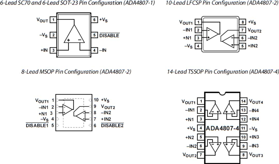
Pin Configurations

Additional Resources
Integration and Collaboration at the Heart of a High Performance Image Sensor Reference Design
In collaboration with Hamamatsu Photonics, Inc., Analog Devices has built a high-performance analog front-end (AFE) board to interface with the Hamamatsu G920x linear array NIR/SWIR InGaAs Image Sensor Family. Image sensors in the 920x family include an integrated Thermoelectric Cooler (TEC) to cool the optical detectors for extremely low noise operation, making them an excellent choice for high-performance NIR/SWIR spectroscopy applications such as gas and mineral identification.
Can You Really Get ppm Accuracies from Op Amps?
There is a march toward 1 ppm accurate systems, especially now that 1 ppm linear ADCs are becoming common. This article presents op-amp accuracy limitations and how to choose the few op-amps that have a chance of 1 ppm accuracy.


