


Microchip Technology PolarFire® FPGA
Microsemi/Microchip PolarFire®现场可编程门阵列 (FPGA) 与同类SRAM FPGA相比,功耗可降低50%。通过12.7Gbps串行器/解串器 (SerDes) 收发器,该款FPGA可为中等密度器件实现低功耗,极为安全可靠。FPGA产品系列特别适用于有线接入网络和蜂窝基础设施、国防和商业航空市场以及工业4.0(包括工业自动化和物联网 (IoT) 市场)等各种应用。
特性
- 成本最优架构
- 面向100K/500K LE器件的架构和过程优化
- 收发器性能优化为12.7Gbps,可减小尺寸
- 1.6Gbps I/O—带CDR的硬化I/O变速逻辑(支持这些GPIO上的SGMII/GbE链路)
- 优于同类的高性能,中档设备中的硬化安全IP
- 功率优化
- 静态功耗为同类竞争设备的1/10
- 收发器性能优化为12.7Gbps,功耗是同类竞争设备的1/2
- 低功耗闪存冻结模式可实现优于同类的待机功耗
- 集成硬IP:DDR PHY、PCIe端点/根端口、加密处理器
- 总功耗:降低达50%
视频
PolarFire FPGA架构

PolarFire FPGA设有高达500K的逻辑单元、12.7G收发器,功耗降低50%。
PolarFire产品系列

PolarFire FPGA有各种器件型号可选,例如收发器设计安全性器件、低功耗收发器器件、收发器数据安全性器件以及收发器设备低功耗数据安全性器件。所有PolarFire FPGA均集成出色的多协议低功耗收发器。低功耗 (L) 器件最多可将静态功耗降低35%。另外,数据安全 (S) 器件集成了DPA安全加密加速器。PolarFire器件目前有扩展商用(0ºC到100ºC)和工业用(-40ºC到100ºC)产品型号可选。
PolarFire Core Family

Microchip PolarFire Core FPGAs bring the power efficiency, security, and reliability of the original PolarFire family to a streamlined platform that eliminates SerDes and PCIe® to reduce cost and complexity for a broad range of applications.
Unlike SRAM-based FPGAs, which are plagued by high static power and configuration volatility, PolarFire Core devices leverage nonvolatile Flash technology for up to 50% lower power consumption, instant-on capability, and built-in resistance to SEUs. This feature makes them excellent options for power- and thermally constrained environments such as industrial control, medical imaging, automotive, and aerospace systems.
小外形尺寸解决方案

Microchip Technology PolarFire® FPGA采用小外形尺寸,适用于中等密度器件。例如,MPF100器件采用11x11mm封装。此外,PolarFire®器件不需要外部配置存储器,而基于SRAM的FPGA通常都会需要。
信息图

评估工具

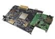
Microchip Technology PolarFire® FPGA视频和图像套件
基于PolarFire® FPGA的高性能图像和视频开发平台。

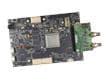
Microchip Technology PolarFire®评估套件
为各类应用提供高性能评估。
Microchip Technology VIDEO-DC-USXGMII FMC子卡
评估和测试四速率PHY IP,与PolarFire ® 视频套件配合使用。
Microchip Technology VIDEO-DC-SDI FMC子卡
评估和测试串行数字接口IP,与PolarFire ® 视频套件配合使用。

Microchip Technology VIDEO-DC-CXP CoaXPress FMC子卡
支持12.5 G CoaXPress PHY,包括即用型参考设计,用于快速进行原型设计。
Related ICs

Microchip Technology MCP16701电源管理集成电路
集成了八个DC-DC降压式稳压器、四个300mA LDO和一个LDO控制器。