


Infineon Technologies PSoC4100S ARM® Cortex®-M0 可编程 SoC
Cypress Semiconductor PSoC4100S ARM® Cortex®-M0 可编程 SoC 是可编程嵌入式系统控制器的可扩展和可重新配置平台架构。 PSoC4100S 将模拟和数字块与灵活的自动路由相结合。 PSoC4100S 将微控制器与标准通信和计时外设相结合。 还结合了电容性触摸传感系统 (CapSense)、可编程通用连续时间和开关电容器模拟模块以及可编程连接。 PSoC4100S 向上兼容 PSoC 4 平台的构件,可以满足新的应用和设计需要。
特性
- 32-bit MCU Subsystem
- 48MHz Arm Cortex-M0+ CPU
- Up to 64KB of flash with read accelerator
- Up to 8KB of SRAM
- Programmable analog
- Two opamps with reconfigurable high-drive external and high-bandwidth internal drive, comparator modes, and ADC input buffering capability
12-bit 1Msps SAR ADC with differential and single-ended modes, and channel Sequencer with signal averaging - Single-slope 10-bit ADC function provided by a capacitance sensing block
- Two current DACs (IDACs) for general-purpose or capacitive sensing applications on any pin
- Two low-power comparators that operate in Deep Sleep low-power mode
- Two opamps with reconfigurable high-drive external and high-bandwidth internal drive, comparator modes, and ADC input buffering capability
- Programmable digital
- Programmable logic blocks allow Boolean operations to be performed on port inputs and outputs
- Low-power 1.71V to 5.5V operation
- Deep sleep mode with operational analog and 2.5µA digital system current
- Capacitive sensing
- Cypress CapSense Sigma-Delta (CSD) provides best-in-class signal-to-noise ratio (SNR) (>5:1) and water tolerance
- Cypress-supplied software component makes capacitive sensing design easy
- Automatic hardware tuning (SmartSense™)
- LCD Drive capability
- LCD segment drive capability on GPIOs
- Serial communication
- Three independent run-time reconfigurable Serial Communication Blocks (SCBs) with reconfigurable I2C, SPI, or UART functionality
- Timing and pulse-width modulation
- Five 16-bit timer/counter/pulse-width modulator (TCPWM) blocks
- Center-aligned, Edge, and Pseudo-random modes
- Comparator-based triggering of Kill signals for motor drive and other high-reliability digital logic applications
- Up to 36 programmable GPIO pins
- 48-pin TQFP, 44-TQFP, 40-pin QFN, 32-pin QFN, and 35-ball WLCSP packages
- Any GPIO pin can be CapSense, analog, or digital
- Drive modes, strengths, and slew rates are programmable
- PSOC Creator Design Environment
- Integrated Development Environment (IDE) provides schematic design entry and build (with analog and digital automatic routing)
- Application Programming Interface (API) component for all fixed-function and programmable peripherals
- Industry-standard tool Compatibility
- After schematic entry, development can be done with Arm-based industry-standard development tools
视频
Block Diagram

Related Products
Infineon Technologies PSoC® 4 ARM® Cortex®-M0微控制器
业界极其灵活且可扩展的低功耗混合信号架构。
Development Tool
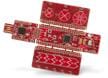
Infineon Technologies CY8CKIT-145-40XX PSoC® CapSense原型开发套件
使设计人员能够使用PSoC 4000S器件评估和开发低功耗CapSense®解决方案。
发布日期: 2017-01-17
| 更新日期: 2025-08-19