



Microchip Technology dsPIC33AK256MPS306 200MHz 32位DSC
Microchip Technology的dsPIC33AK256MPS306 200MHz 32位数字信号控制器 (DSC) 附带32/64位浮点单元 (FPU)、可达256KB的闪存程序存储器和64KB SRAM数据存储器,采用小占位面积封装(36/48/64引脚,VQFN/TQFP),适用于空间受限的设计。40MSPS高速12位ADC,100MHz高带宽低输入电压偏移运算放大器,5ns快速比较器,高速PWM输出,专为下一代服务器电源、工业自动化、先进传感、触摸控制和电机控制应用而设计。
Microchip dsPIC33AK256MPS306具有硬件加密加速器,并支持后量子密码学 (PQC)。该系列产品按照ISO 26262和IEC 61508功能安全符合标准设计,支持AEC-Q100认证。
特性
- 工作条件
- 3.0V至3.6V:-40°C至+85°C,DC到200MHz
- 3.0V至3.6V:-40°C至+125°C,DC到200MHz,计划了认证
- 3.0V至3.6V:-40°C至+150°C,DC到200MHz,计划了认证
- 高性能DSP CPU
- 32位富指令集让速度和程序代码大小得到了优化
- 兼容16位dsPIC33内核
- 非分页线性数据/闪存24位寻址空间
- 16位/32位指令,可优化代码尺寸和性能
- 32位宽数据路径
- 单精度和双精度浮点运算单元 (FPU) 协处理器
- 2kbyte指令缓存
- 16个32位工作寄存器
- 双72位累加器,支持32位和16位定点DSP运算
- 八级深度工作寄存器集
- 八级深累加器寄存器集
- 八级深度浮点寄存器集
- 32位富指令集让速度和程序代码大小得到了优化
- 存储器
- 可达256Kbyte的程序闪存
- 10,000次擦除/写入周期耐久性
- 最少20年数据保留时间
- 在软件控制下可自编程
- 可编程代码保护
- 闪存纠错码 (ECC)
- 双闪存面板
- 支持实时更新
- 可编程OTP区域
- 通过ICSP™写入抑制保护整个Flash OTP区域
- 单独的64x128位OTP
- 可达64Kbyte的静态RAM
- RAM错误纠正码 (ECC)
- RAM存储器内置自检 (MBIST)
- 可达256Kbyte的程序闪存
- 安全
- 通过ICSP写入抑制保护Flash OTP区域
- 片上安全启动Flash可配置为不可变信任根,保有Flash存储器的部分区域可配置为OTP区域
- 功能包括
- 通过主机代码映像验证和主机代码签名支持安全启动
- 支持主机代码的安全更新:安全加密密钥储存和映像解密
- X.509证书储存、解析、验证和吊销,支持ECC和RSA
- 识别用的128位唯一设备序列号 (UUID)
- 支持安全用例
- 安全启动
- 密钥储存在IRT/不可变安全启动区实现
- 安全启动
- 安全FirmWare更新
- 安全调试
- 闪存保护
- 在闪存地址范围内多达八个闪存保护区域的配置
- 区域可以配置为
- 不可变信任根 (IRT)
- OTP区域
- R/W/X(读/写/执行)保护的组合
- 区域可以:
- 做成永久化
- 设备重置前锁定
- 执行代码期间启用/禁用
- 闪存保护区域可以应用于活动分区、非活动分区或同时应用于两者。
- 密码加速器模块 (CAM)
- AES-128、AES-192和AES-256(完全符合NIST FIPS 197标准)
- ECB、CBC、CFB、OFB、CTR、GCM、CCM、XTS、CMAC模式
- AES-128、AES-192和AES-256(完全符合NIST FIPS 197标准)
- HASH/MAC
- SHA3-224、SHA3-256、SHA3-384、SHA3-512、SHAKE128和SHAKE256能力
- SHA-1、SHA-256、SHA-224、SHA-384和SHA-512能力
- RSA、DSA和ECC公钥加密
- 利用/不利用中国剩余定理 (CRT) 的RSA,密钥长度可达4096位
- 质数域P-192、P-224、P-256、P-384、P-521
- 二进制域K-163、K-233、K-283、K-409、K-571
- 二进制域B-163、B-233、B-283、B-409、B-571
- P-224、P-256、P-384和P-521椭圆曲线——ECDSA签名/验证
- DSA支持密钥长度最可达2048位
- ECDH支持P256和P224曲线
- 支持SECP256K1(比特币/区块链曲线)ECDSA
- 支持256位Brainpool椭圆曲线——ECDSA、ECDH
- 椭圆曲线Diffie-Hellman (ECDH/ECDHE) 密钥协商
- 利用/不利用中国剩余定理 (CRT) 的RSA,密钥长度可达4096位
- 符合NIST-800-22和NIST-800-90B标准的真随机数生成器 (TRNG)
- 通过ICSP写入抑制保护Flash OTP区域
- 高分辨率PWM
- 多个PWM生成器包括四对(八个输出)生成器,精细边沿位置(FEP)分辨率低至78ps
- 上升和下降沿死区时间
- 死区时间补偿支持更低速度操作
- 用于高频工作的时钟斩波
- PWM支持
- BLDC、PMSM、ACIM、SRM和步进电机
- 恒定导通时间、滞回、突发模式电源应用
- 故障和电流限制输入
- 为ADC触发提供灵活的触发器配置
- 高速模数转换器
- 三个12位分辨率SAR ADC
- 每个ADC的转换速率可达40Msps
- 可达14个模拟输入引脚
- 16位采样能力
- 16个设置通道,每个通道均可
- 分配给任何模拟输入(I/O引脚或内部信号)
- 设置为不同的采样时间
- 可配置为单端或差分
- 转换结果可以为无符号或有符号格式
- 转换结果可以设置为左对齐(分数格式)
- 具有独立的32位转换结果寄存器
- 支持四种采样模式
- 多个样本的过采样
- 多个样本的集成
- 窗口(门信号有效时累积的多个样本)
- 单一转换
- 所有通道均设有数字比较器,用于检测可配置的阈值
- 最后三个设置通道设有第二个结果累加器,用于实现二阶滤波器
- 外设
- 三个4线SPI模块(可达50Mbps)
- 32字节FIFO
- 可变数据宽度
- I2S模式
- 多通道数字音频接口(I2S)
- 三个156kSPS支持16位分辨率音频采样率的ADC
- 启用DMA的实时音频串流(提供有八个DMA通道)
- 支持TDM4/8/16/32,和DMA外设使用收发帧同步脉冲的SPI模式
- 用于语音和声学处理的音频DSP
- 两个I2C模块,支持地址掩码和IPMI
- 一个I3C模块,具有主控制器和从控制器模式,以及I3C/I2C目标能力
- 四个协议UART,具有8字符RX/TX FIFO,并支持自动处理
- LIN 2.2
- DMX
- 智能卡 (ISO 7816)
- IrDA®
- 两个SENT模块
- 三个专用32位定时器/计数器模块
- 输出捕获/比较/PWM/定时器模块
- 一个MCCP
- 四个SCCP
- 可灵活配置为PWM、输入捕获、输出比较或定时器
- 每个模块中两个16位定时器或一个32位定时器
- 8通道硬件直接存储器访问 (DMA) 模块
- 一个正交编码器接口 (QEI) 模块,带四个输入(Phase A、Phase B、Home和Index)
- 串行编码器BiSS接口,最多支持四个客户端编码器
- 四个可配置逻辑单元 (CLC),内部连接用于选择外设和PPS(每秒脉冲)
- 外设触发信号生成器 (PTG)
- 16个可能的触发源用于其他外设模块
- 基于不相干CPU的状态机的指令排序器
- 一个CAN FD模块
- 集成触摸控制器 (ITC) 模块
- 先进的电容感应、触摸按钮、滑块和滚轮
- 多达24个自电容通道和多达72个互电容通道
- 一个旋转变压器信号转数字信号转换器 (RDC) 模块
- 三个4线SPI模块(可达50Mbps)
- 控制器
- 大电流I/O灌/拉能力
- 可编程弱上拉和下拉电阻器
- 可编程开漏输出
- I/O引脚上边沿或电平变化通知中断
- 外设引脚选择 (PPS) 可重新映射引脚,用来减少电路板布局的复杂性
- 多个中断矢量,具有单独可编程优先级
- 五个外部中断引脚
- 可选择的振荡器选项,包括
- 8MHz、0ºC至85ºC时1%精度的内部快速RC(FRC)振荡器
- 8MHz、2%精度内部备用快速RC(BFRC)振荡器带32kHz分频器输出
- 高速晶体谐振器振荡器或外部时钟
- 两个1.6GHz PLL,它们可以从FRC或晶振加时钟脉冲
- 参考时钟脉冲输出 (REFO)
- 低功耗管理模式(睡眠和空闲)
- 上电重置和掉电重置
- 板载1.1V降压稳压器,为内核电压供电
- 模拟
- 可达五个5nS含12位PDM DAC的模拟比较器
- 输入多路复用
- 斜坡补偿
- 可达两个DAC输出缓冲器
- 三个轨至轨100MHz运算放大器具有
- 40V/μS转换速度
- 1mV偏移(典型值),带校准功能
- VREF/2输出可用于运算放大器输入偏置
- 四个10µA恒流源,四个可编程电流源
- 集成触摸控制器
- 与ADC处理能力无干
- 支持自电容CVD(电容式分压器)和互电容CVD触控模式
- 11到24个触控ADC RX输入
- 9到15个触控TX输出
- 可达五个5nS含12位PDM DAC的模拟比较器
- 安全
- 窗口Watchdog定时器 (WDT)
- Deadman定时器 (DMT)
- 八个I/O完整性监视器 (IOIM)
- 故障安全时钟监视器 (FSCM),具有自动切换到备用时钟源的功能,并具有可编程的过频/欠频阈值
- 闪存纠错码 (ECC)
- RAM错误纠正码 (ECC)
- RAM存储器内置自检 (MBIST)
- 32位循环冗余校验 (CRC) 模块
- ICSP写入抑制保护整个Flash OTP区域
- 内部稳压器
- 虚拟PPS引脚,用于冗余和监控
- 温度传感器二极管
- 内核电压电源监控器,具有可配置的故障注入
- 功能安全
- 目标
- ISO 26262 ASIL B
- IEC 61508 SIL 2
- IEC 60730 Class B
- 符合ISO 26262和IEC 61508标准的设备开发
- 目标
应用
- 功率因数校正(PFC)
- 交错PFC、图腾柱PFC
- 临界导通PFC
- 多级飞跨电容器PFC
- 直流-直流转换器
- 降压、升压、正激、反激、推挽
- 半桥/全桥
- 相移全桥
- 谐振转换器
- DC-AC
- 半桥/全桥逆变器
- 谐振逆变器
- 电机控制
- BLDC
- PMSM
- SR
- ACIM
- 高级传感器接口
- 高性能嵌入式控制
- 高速数据采集和处理
- 安全关键型设计
- 数字照明
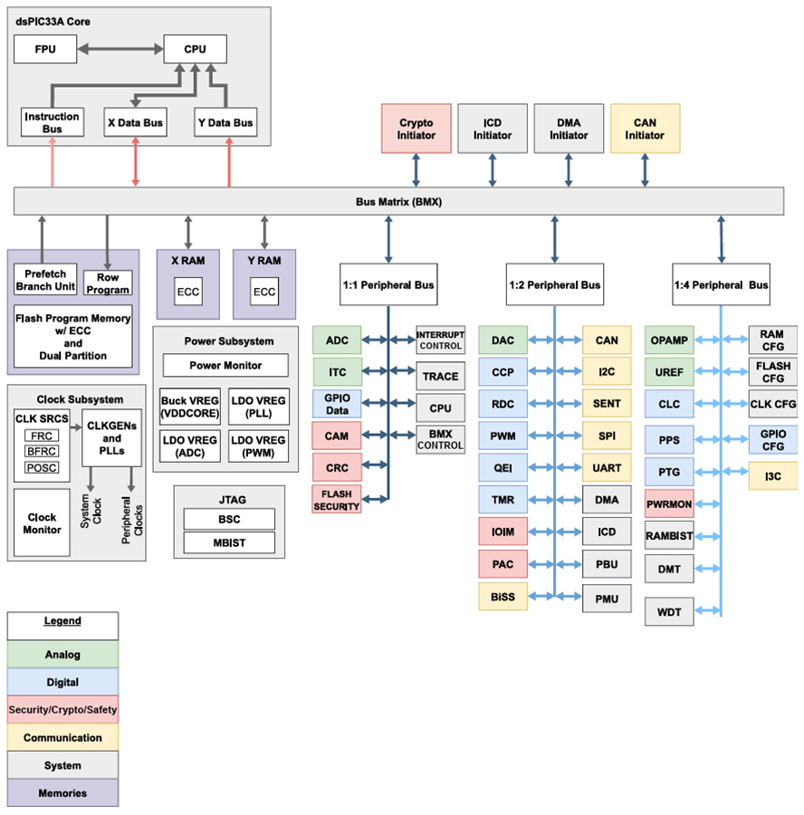
方框图
相关数字信号控制器

Microchip Technology dsPIC33AK数字信号控制器 (DSC)
设计用于高性能和实时精密控制应用。
开发工具
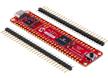
Microchip Technology EV17P63A Curiosity Nano评估套件
一款让32位dsPIC33A数字信号控制器 (DSC) 的评估和采用很容易的高性价比评估板。
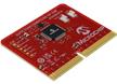
Microchip Technology dsPIC33AK256MPS306通用DIM (EV02E57A)
演示dsPIC33AK256MPS306系列数字信号控制器 (DSC) 的能力。
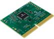
Microchip Technology dsPIC33AK256MPS306电机控制DIM (EV22K90A)
用于评估用在电机应用上的整个dsPIC33AK256MPS306 DSC系列。

Microchip Technology dsPIC33AK512MPS506数字电源即插即用模块 (PIM)
展示dsPIC33AK512MPS506数字信号控制器 (DSC) 的功能。

Microchip Technology MPLAB® PICkit™5内电路调试器/编程器
能够对所有Microchip元器件进行快速原型设计和便携的、生产就绪的编程。

Microchip Technology MPLAB® PICkit™ Basic调试器
非常适合用于不需要高压编程或高级调试功能的项目。
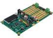
Microchip Technology dsPIC33A数字电源入门套件4
数字电源套件,配备降压与升压级、板载负载、编程及调试功能。
View Results ( 4 ) Page
| 物料编号 | 数据表 | 封装 / 箱体 | 接口类型 | 计时器/计数器数量 |
|---|---|---|---|---|
| dsPIC33AK256MPS306-E/M7 |  |
VQFN-64 | I2C, CAN, SPI, UART | 3 x 32 bit |
| dsPIC33AK256MPS306-I/M7 | |
VQFN-64 | I2C, SPI | 3 Timer |
| dsPIC33AK256MPS306-I/PT | |
TQFP-64 | I2C, CAN, SPI, UART | 3 x 32 bit |
| dsPIC33AK256MPS306-E/PT | |
TQFP-64 | I2C, CAN, SPI, UART | 3 x 32 bit |
发布日期: 2026-07-07
| 更新日期: 2026-09-03