Altera SoC FPGA 系列
Altera SoC FPGA 集成了由处理器、外设以及存储器接口组成的基于 ARM 的硬核处理器系统(HPS),并采用了高带宽互连背板。该系列器件兼具硬核知识产权(IP)的高性能、低功耗和可编程逻辑的灵活性等优点。该系列基于 ARM 的 SoC FPGA 可由用户进行自定义,特别适用于通过在单个FPGA中集成分立处理器和数字信号处理(DSP)功能实现降低系统功耗、压缩成本、缩小电路板大小等目标的应用场合。它们可通过定制硬件和软件,并为FPGA添加对几乎所有接口标准或协议的支持功能,实现最终产品的差异化。Altera SoC FPGA 通过对实际应用中的硬件和软件进行升级,不但可延长产品寿命,而且可提高收益。它们还可通过处理器和FPGA之间的高带宽互联提升系统性能。该系列器件分别属于不同的 Cyclone® V和Arria® V FPGA 系列,共有数十种型号,且包括 PCI Express® Gen2、多端口存储器控制器以及高速串行收发器等附加硬逻辑。SoC FPGA 采用了 TSMC 的28nm低功耗(28LP)工艺,在降低了功耗和成本的同时实现了成本敏感型应用所需的性能等级。Altera SoC FPGAs extend product life and revenue through hardware and software updates in the field. They also improve system performance via a high-bandwidth interconnect between the processor and the FPGA. These devices join the diverse family of Cyclone® V and Arria® V FPGAs with dozens of devices and variations and include additional hard logic such as PCI Express® Gen2, multiport memory controllers, and high-speed serial transceivers. Built on TSMC's 28nm Low-Power (28LP) process, the SoC FPGAs drive down power and cost while enabling performance levels required by cost-sensitive applications.
特性
- Processor Architecture
- Dual-core Arm Cortex-A9 MP core processor
- Up to 800MHz maximum frequency
- Support for symmetric multiprocessing (SMP) and asymmetric multiprocessing (AMP)
- Each processor core includes:
- 32KB of L1 instruction cache
- 32KB of L1 data cache
- NEON media processing engine
- Single- or double-precision floating-point unit
- Memory management unit (MMU)
- Private interval timer
- Private watchdog timer
- 512KB of shared level 2 (L2) cache
- SCU for cache coherency
- Accelerator coherency port (ACP)
- Global timer
- Generic interrupt controller
- CoreSight™ instruction trace
- Dual-core Arm Cortex-A9 MP core processor
- Memory Interface Support
- Multiport SDRAM controller subsystem
- DDR2 and DDR3
- LPDDR1 and LPDDR2
- Error correction code (ECC)
- Flash memory controller
- NAND with direct memory access (DMA) and optional ECC
- Quad SPI (NOR)
- Secure Digital (SD)/ secure digital I/O
- (SDIO)/ MultiMediaCard (MMC) with DMA
- Multiport SDRAM controller subsystem
- Interface Peripherals
- 2x 10/100/1000Mbps Ethernet media access controllers (EMACs) with DMA
- 2x USB 2.0 On-The-Go (USB OTG) controllers with DMA
- 4x I2C controllers
- 2x controller area networks (CAN), 2x master SPIs, 2x slave SPIs, UART
- Up to 71x general-purpose I/Os (GPIOs) and 14x input-only
- On-chip memory
- 64KB on-chip RAM
- 64KB on-chip boot ROM
- Debug
- IEEE standard 1149.1-2001 (JTAG)
- CPU Debug Access Port (DAP)
- Direct memory debug via Advanced High-performance Bus Access Port (AHB-AP)
- Embedded trace router (ETR) port with DMA
- Processor trace
- System bus trace
- Operating system (OS) trace
- On-chip trace storage
- IEEE standard 1149.1-2001 (JTAG)
- System Peripherals
- 4x general-purpose timers
- 2x watchdog timers
- 8-channel DMA controller
- FPGA manager for FPGA configuration
- Clock and reset managers
- HPS/FPGA interfaces
- HPS-to-FPGA bridges
- Processor and DMA access to FPGA peripherals
- Configurable 32-, 64-, or 128-bit Advanced Microcontroller Bus Architecture (AMBA®) Advanced eXtensible Interface (AXI™)
- FPGA-to-HPS bridges
- FPGA masters access processor subsystem peripherals
- Configurable 32-, 64-, or 128-bit AMBA AXI interface
- Coherent access to processor cache through ACP
- FPGA-to-HPS SDRAM controller subsystem interface
- FPGA access to DRAM for shared memory
- Up to 6x masters, 4x 64-bit read, 4x 64-bit write data
- Miscellaneous
- FPGA-to-HPS interrupts
- DMA handshake (allows FPGA peripherals to perform block-level transfers with system DMA controller)
- More than 100Gbps HPS-to-FPGA and FPGA-to-HPS bandwidth
- HPS-to-FPGA bridges
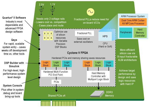
Cyclone V System Level Cost Savings Through Integration

Reducing Total System Cost Through Integration
Because Cyclone V integrates an abundance of hard intellectual property (IP) blocks, the user can differentiate and do more with less overall system cost, power, and design time. Key hard IP blocks include the following:
• Hard memory controllers supporting 400MHz DDR3 SDRAM with optional error correction code (ECC) support
• PCI Express® (PCIe®) Gen2 with multifunction support
• Variable-precision digital signal processing (DSP) blocks
• HPS Dual-core ARM Cortex-A9 MPCore processor


