


Monolithic Power Systems (MPS) MP2760 Battery Management Buck/Boost Charger ICs
Monolithic Power Systems (MPS) MP2760 Battery Management Buck/Boost Charger ICs are designed for battery packs with 1 to 4 cells in series and accept a wide 4V to 22V input voltage (VIN) range to charge the battery. The buck-boost topology allows a battery voltage above or below VIN. The TQFN-30 (4mm x 5mm) packaged MP2760 ICs provide narrow-voltage DC (NVDC) power path management. For safe operation, the devices limit the die temperature o a configurable threshold. Other safety features include input over-voltage protection (OVP), battery OVP, system OVP, thermal shutdown, and a configurable timer to prevent prolonged charging of a dead battery.
When the input is present, the MPS MP2760 operates in charge mode. The device measures the battery voltage and charges the battery with four phases: constant current trickle charge, constant current pre-charge, constant current fast charge, and constant voltage charge. Additional features include charge termination and automatic recharge. Charge and discharge parameters can be configured via the I2C/SMBus interface, while the I2C/SMBus registers provide statuses and fault information.
Features
- Buck-Boost charger for 1 to 4 cells in series battery pack
- 4V to 22V input voltage (VIN)
- Up to 26V sustainable voltage (Up to 28V with external MOSFET)
- Supports USB 2.0, USB 3.0, USB 3.1, USB 3.2, Type-C, and USB PD 3.0 settings
- Smooth transition for Buck and Boost mode
- Configurable Maximum Input Current (IIN) limit and minimum VIN limit
- Up to 6A configurable charge current
- Configurable battery-full voltage up to 4.68V/cell with 0.5% accuracy
- Configurable 3V to 21V output voltage (VOUT) with 20mV/step
- Compatible with USB PD 3.0
- Up to 6A output current with 50mA/step 500kHz to 1.2MHz configurable fSW
- I2C or SMBus host control interface
- Input power source status indication pin
- Integrated 10-Bit ADC for monitoring
- Analog output pin to monitor battery current in Charge/Source Mode
- Input Over-Voltage Protection (OVP), System OVP, and Battery OVP
- System SCP in Charge Mode
- Output SCP in USB PD Source Mode
- Battery missing detection
- NTC Pin floating detection
- Integrated N-Channel MOSFET for input power pass-through or OVP
- Integrated N-Channel MOSFET for NVDC power path control
- Configurable battery temperature protection threshold, compliant with JEITA
- Thermal regulation/shutdown
- Available in a TQFN-30 (4mm x 5mm) package
Applications
- Ultrabooks, notebooks, and tablets
- USB PD devices
- General multiple-cell applications
Specifications
- Recommended operating conditions
- 4V to 22V supply voltage (VIN)
- Up to 6A input current (IIN)
- Up to 6A system current (ISYS)
- Up to 6A charge current (ICC)
- Up to 18.72V battery voltage (VBATT)
- -40°C to +125°C operating junction temperature range
- 3.29W continuous power dissipation at +25°C
- ±0.5µA pin leakage current
- +150°C typical thermal shutdown rising threshold
- +20°C typical thermal shutdown hysteresis
- +120°C typical thermal regulation threshold
- Analog-to-Digital Converter (ADC)
- 50kHz typical sample rate
- 1.8V typical ADC reference
- 10-bit ADC resolution
- 10kHz to 400kHz SMBus clock frequency range
- ESD ratings
- 2kV Human Body Model (HBM)
- 750V Charged Device Model (CDM)
Associated Dev Tools

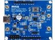
Monolithic Power Systems (MPS) EV2760-VT-00A Evaluation Board
Demonstrates the features of the MP2760 ICs in a TQFN-30 (4mm x 5mm) package.

Monolithic Power Systems (MPS) MP2760 Evaluation Kit
Used to evaluate the MP2760 versatile buck-boost NVDC charger IC.
Monolithic Power Systems (MPS) MEZS7-PDCharger-MP2760 Solution Module
Designed for dual-role port (DRP) applications.
Typical Application
 MP2760 Battery Management Buck/Boost Charger ICs")
Block Diagram
 MP2760 Battery Management Buck/Boost Charger ICs")